Wire Bonding
Interconnecting integrated circuits for die-level attachment.
Wire bonding is one of the most commonly used methods for die-level attachment in printed circuit boards and microelectronic packaging.
Wire bonding is the primary interconnect method for semiconductor die (chip) to a component lead-frame, PCB, and other die (chip-to-chip). This technique involves the use of thin wires, commonly made of gold, aluminum, or copper, to establish electrical connections between the pads on an IC substrate or lead frame.
Do you see the wirebonds?
The image below shows an optically clear LED package used in electronics assembly.

Wire Bond History at Analog Technologies
Analog Technologies has over 25 years of experience with wire bonding.
During the initial years of the company (1993), we were principally focused in electronics design. Our designs involved complex and high-performance circuitry using advanced packages. We started assembling our products because we could not find suppliers to support our complex, low-volume production orders. This ultimately launched our electronic manufacturing services business.
In the late 1990’s, a customer needed high-performance circuitry in a very small area of a PCB. Analog Technologies invested in a wedge bonder and developed processes to wire bond an integrated circuit chip directly to the PCB (Chip On Board (COB)).
Over the last two decades, ATC added several pieces of semiconductor die-processing equipment, including:
-
Semi and Fully Automatic Ball Bonders
-
Semi-Automatic Die Attachment for Eutectic Solders and Adhesives
-
Plasma Chamber
-
Wire Bond Pull Tester
-
Die Shear Tester
-
Clean Room
Our wire bonding capabilities include thermocompression ball bonding (TC), ultrasonic (US) wedge bonding, and thermosonic (TS) ball bonding. Wire sizes can vary by method, metal type, and connection requirements, but can vary anywhere between 15 µm (0.6 mils) to 500 µm (20 mils). Typical wire materials include Gold (Au) and Aluminum (Al).
What's Inside The IC?
The image below shows a common SOIC-8 package used in PCBA assembly

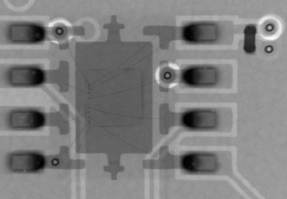
Below is that same SOIC-8 package shown under an XRAY

(1) LEAD FRAME:
The internal die is attached to the lead frame by wire bonds.
(2) DIE:
The internal die is attached to the lead frame by wire bonds
(3) WIRE BONDS:
Each thin line going from the die to the lead frame represents a wire bond.
To this day, what differentiates Analog Technologies is the ability to understand customer requirements, high-performance electronics, design for manufacturing, manufacturing methods, and offer solutions. Analog Technologies routinely develops custom methods and processes to solve customer assembly challenges. With justification, Analog Technologies will also invest in capital equipment to manufacture these products. The foray into wire bonding in the late 1990’s is an example of the collaborative, solutions-oriented approach Analog Technologies is willing to take.
Ask how Analog Technologies can help with your PCBA and die-level assembly challenges: Contact Us
